
Materials Science
Semiconductor Materials
Time-resolved spectroscopy of semiconductor materials
Charge carrier dynamics in semiconductors are determined by the architecture and function of the respective device. Thus directly reflecting the nature and quality of wafer materials. Understanding these critical parameters in semiconductor photophysics is of the utmost importance. A precise and efficient measurement of the diffusion lengths of photo-excited electrons and holes is essential for characterizing these systems. Time-resolved photoluminescence quenching experiments are a valuable tool for determining such diffusion lengths.
For specific classes of semiconductors, the characteristic charge carrier lifetime depends strongly on the nature and dimensions of the materials and interfaces involved. Furthermore, surface effects, passivation, energy transfer efficiency of sensitizers as well as the presence of dopants, impurities, and defect sites can also introduce significant variations in the observed lifetimes.
As photoluminescence behavior of a semiconductor is a direct monitor for its charge carrier dynamics, time-resolved photo-luminescence (TRPL) via time-correlated single photon counting (TCSPC) is well suited for analyzing phenomena that influence its dynamics. As a result, the phenomena occurring within a particular system can be characterized directly down to the sub-nanosecond time scale.
 Contact us
Fast charge carrier dynamics in semiconductors can be sutdied using various types of set-ups. These can be divided into three broad categories: spectrometers, confocal microscopes, or a combination of both spectrometer and microscope.
Generally speaking, the measurements work by exciting the semiconductor via a pulsed light source. The emitted signal is then separated from the excitation light thorugh filters or monochromators before being collected by a single photon sensitive detector and processed by a Time-Correlated Single Photon Counting (TCSPC) unit.
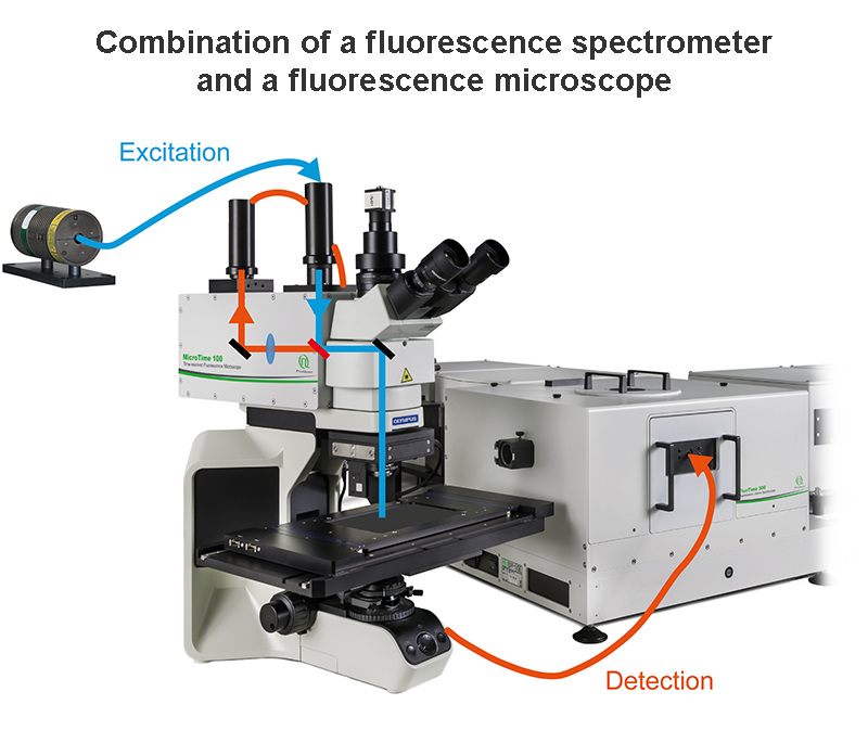
The main difference between the set-ups outlined above lies in the addtional information they collect. A spectrometer equipped with a good monochromator will also provide high spectral reslution, while a microscope gives good spatial resolution. A combined system offers the best from both world by collecting time, spectral, and spatial information from a sample.
Consequently the essential components of a set-up suited for studying semiconductor dynamics are:
- pulsed excitation source (diode laser, LED or multi-photon excitation system)
- means of separating excitation from luminescence (monochromator or filters)
- single photon sensitive detector
- TCSPC unit to process lifetime data


PicoQuant offers these system for studying semiconductor materials:
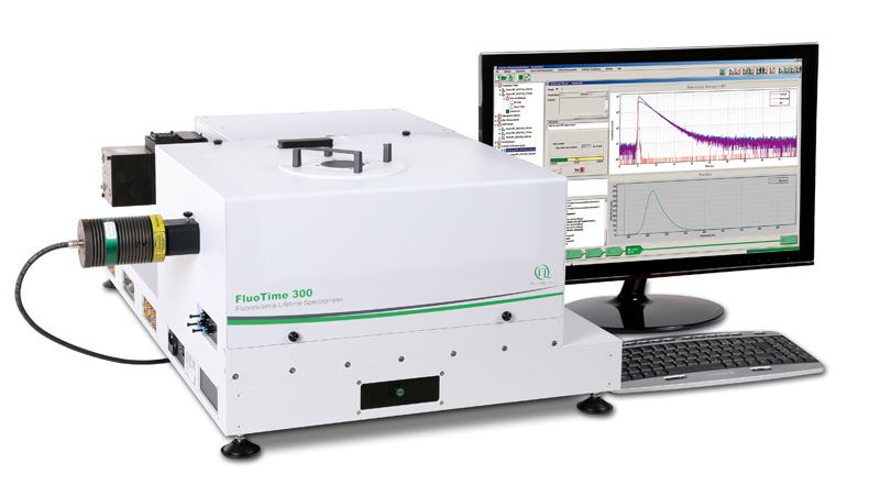
 FluoTime 300
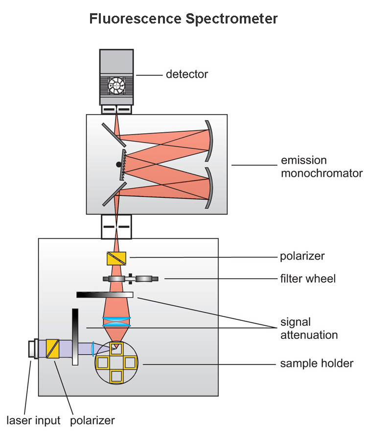
Fully Automated High Performance Fluorescence Lifetime Spectrometer
The FluoTime 300 "EasyTau" is a fully automated, high performance fluorescence lifetime spectrometer with steady-state and phosphorescence option. It contains the complete optics and electronics for recording fluorescence decays by means of Time-Correlated Single Photon Counting (TCSPC) or Multichannel Scaling (MCS). The system is designed to be used with picosecond pulsed diode lasers, LEDs or Xenon lamps. Multiple detector options enable a large range of system configurations. With the FluoTime 300 decay times down to a few picoseconds can be resolved.
 MicroTime 100
Upright time-resolved confocal microscope
The MicroTime 100 is an idea tool for the study of time-resolved photoluminescence of solid samples such as wafers, semiconductors or solar cells. It can also be used for mapping purposes or to measure intensity dependent TRPL. The system is based on a conventional upright microscope body that permits easy access to a wide range of sample shapes and sizes. The MicroTime 100 can be supplied with either manual scanning or with a 2D piezo scanner with either µm or cm resolution.
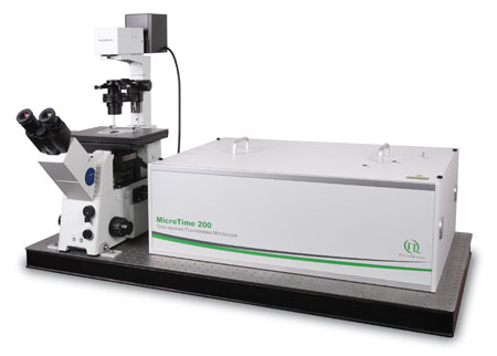
 MicroTime 200
Time-resolved Confocal Fluorescence Microscope with Unique Single Molecule Sensitivity
The MicroTime 200 time-resolved fluorescence microscope system is a powerful instrument capable of Fluorecence Corelation Spectroscopy and its daughter techniques as well as Fluorescence Lifetime Imaging (FLIM) with single molecule detection sensitivity. It contains the complete optics and electronics for recording virtually all aspects of the fluorescence dynamics of microscopic samples or femtoliter volumes. The instrument gains its exceptional sensitivity and flexibility in combination with unprecedented ease-of-use from a unique fusion of miniaturized and highly sophisticated state-of-the-art technologies. Although, these technologies enable to run an instrument of comparable complexity and power without having to spend more time on instrument maintenance than on original scientific content, the MicroTime200 remains an open platform that allows the advanced scientist to easily built upon the open character of the instrument in order to realize highly customized applications
The following core components are needed to build a system capable of investigating charge carrier dynamics in semiconductors, which are (partly) available from PicoQuant:
- Laser drivers
- Laser or LED heads
- Photon Counting Detector
- UV/Vis sensitive PMA Hybrid Series
- UV/Vis sensitive Photomultiplier Detector Assembly
- NIR sensitive NIR Photomultiplier Detector
- TCSPC and MCS Electronics
- Analysis software
- Monochromator or excitation cut-off filters
- Confocal or focussing and collection optics
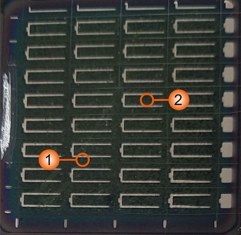
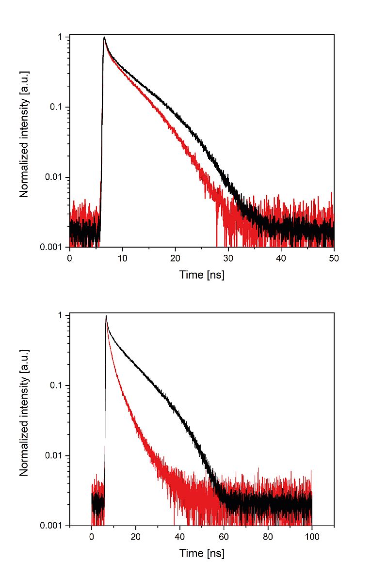
Studying the photoluminescence of a CIGS based solar cell
") In this example, steady state and time-resolved spectra from a Copper Indium Germanium diSelenide (CIGS)-based solar cell have been measured. The cell is built up as a stack starting with a Mo back contact, followed by a 1.5 µm thick CIGS layer, a 50 nm CdSe buffer layer, a 150 nm iZnO layer and topped off with a 300 nm thick ITO contact. A silver grid is layered over the top contact (see Figure 5). Steady-state emission spectra and photoluminescence decays were recorded from two spots: one close to a silver grid line and the other roughly in the middle between two lines.
In this example, steady state and time-resolved spectra from a Copper Indium Germanium diSelenide (CIGS)-based solar cell have been measured. The cell is built up as a stack starting with a Mo back contact, followed by a 1.5 µm thick CIGS layer, a 50 nm CdSe buffer layer, a 150 nm iZnO layer and topped off with a 300 nm thick ITO contact. A silver grid is layered over the top contact (see Figure 5). Steady-state emission spectra and photoluminescence decays were recorded from two spots: one close to a silver grid line and the other roughly in the middle between two lines.
Steady state and time-resolved data was recorded using a FluoTime 300 spectrometer equipped with the FluoMic add-on and a 560 nm ps pulse laser source for excitation. The sample was observed either through a 20x or 40x objective, leading to ca. 60 µm excitation spot size and about 10 µm detection area for the 20x objective, and ca. 30 µm (excitation) and 5 µm (detection) for the 40x objective.
 The emission spectra recorded at both spots are identical: a broad, featureless band with a maximum at 1250 nm and arenot influenced by a change in objective. However, the luminescence decays recorded at 1250 nm are significantly affected. The difference is even more pronounced at position two, where not only the average lifetime is quite shorter, but also the shape of the decay curve changes massively.
Set-up:
- FluoTime 300 equipped with the FluoMic add-on
- Excitation: 560 nm using a VisUV-560 laser module
Sample courtesy of Dr. G. Brammertz, IMEC, Leuven (Belgium)
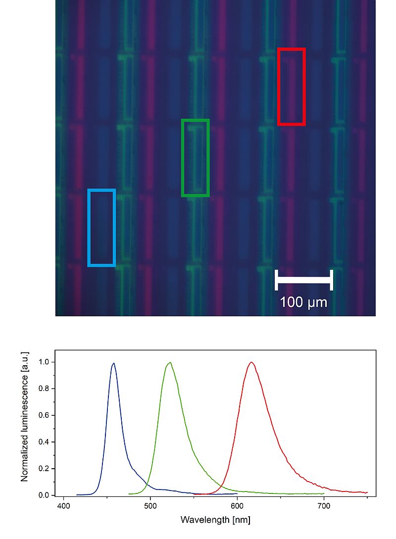
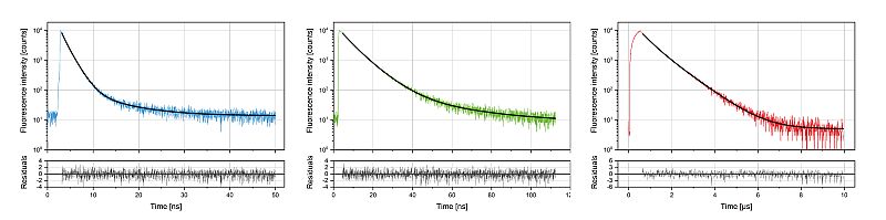
Investigating pixels on a LED display
 For this example, we placed a regular smartphone on the stage of an Olympus BX43 upright microscope to acquire steady-state as well as time-resolved data from individual pixels of its screen using the FluoMic add-on for the FluoTime 300. The microscope stage can accommodate even rather large or unconventionally shaped objects.
The microscope stage was used to move a white part of the screen into the 20x objective’s focal point. The detection spot was then moved to either a blue, green, or red pixel where the corresponding emission spectra and luminescence decay curves were acquired. The sample was excited at 440 nm using a ps pulsed diode laser from PicoQuant. Luminescence decay of blue pixels was acquired at 460 nm, green pixels at 522 nm, and red pixels at 620 nm, respectively. It should be mentioned that the laser was used in burst mode (100 kHz effective repetition rate, 500 ns burst length) when luminescence kinetics of red pixels was collected.
 Set-up:
- FluoTime 300 equipped with the FluoMic add-on
- Excitation: 440 nm ps pulsed laser head from the LDH Series
Determining electron-hole diffusion lengths in perovskite solar cells
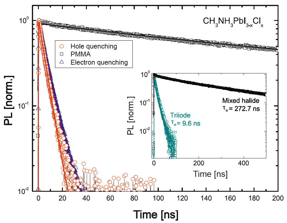
 The example shows data obtained from mixed halide and triiodide organometal perovskite layers in presence of either an electron (blue) or hole (red) quenching layer, or a PMMA coating (black). The decay curves were recorded at 780 nm, corresponding to the peak emission of both materials. The measured decay dynamics can be fitted to a diffusion model, allowing to derive diffusion lengths. Here, the diffusion length of the electrons and holes in the mixed halide perovskite was 1 μm while the triiodide material featured a much shorter length of 100 nm, correlating well with performance of these materials as solar cells.
Set-up:
Reference: S. D. Stranks et al., Science, 342 (2013), p.341
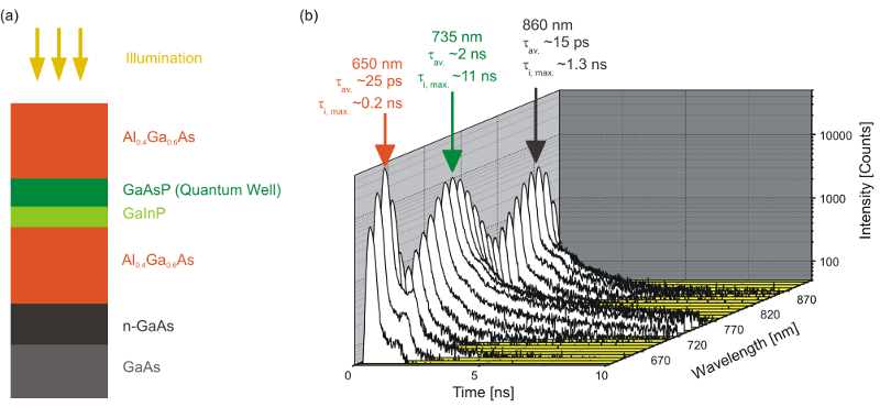
TRPL of a GaAsP quantum well system
 Transient TRPL spectrum of a quantum well structure illuminated at 595 nm and measured with a fluorescence lifetime spectrometer showing (a) the layer structure of the quantum well and (b) the time-resolved emission spectrum (TRES) from the wafer. The emission peak at 650 nm stems from the Al0.4Ga0.6As-barrier, the band around 735 nm from the GaAsP quantum well and the peak at around 860 nm from the n-GaAs layer and the GaAs substrate. The decays recorded for each spectral channel can be well described with a three-component exponential model. Only the average lifetime and longest component of the fits are displayed. The measurement exemplifies the correlation of characteristic charge carrier dynamics in material specific spectral channels of the multi-component system.
Set-up:
- FluoTime 300
- Excitation: 595 nm using a LDH-P-FA-595 laser head and a PDL 800-D driver
- Analysis: EasyTau 2
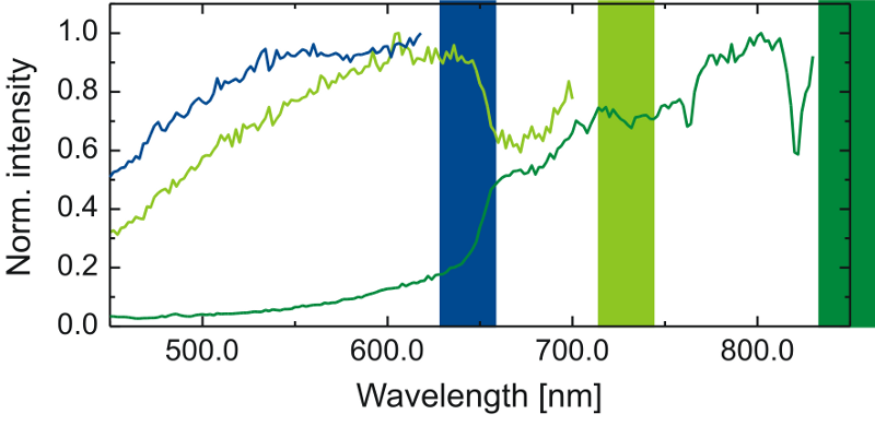
 This figure shows excitation spectra that were recorded at three different wavelengths: one at 650 nm corresponding to the peak of the Al0.4Ga0.6As-barrier (blue); the second at 735 nm which is due to the quantum well layer (light green); the third at 860 nm that is associated to the n-GaAs-layer and GaAs substrate (dark green). The spectrum of the quantum well layer shows a prominent drop in intensity around 650 nm indicating an interaction with the barrier layer. The n-GaAs-layer and GaAs substrate on the other hand show an increase in intensity around 650 nm, which correlates with the absorption edge in the barrier at wavelengths longer than the barrier band gap. The rectangles illustrate the band gaps of the corresponding layers.
Set-up:
- FluoTime 300
- Excitation: CW Xe lamp
- Detection: 650, 735, and 860 nm
- Analysis: EasyTau 2
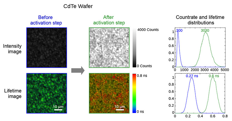
CdTe-polycrystalline wafer surface
 A CdTe-polycrystalline wafer surface was scanned on a confocal microscope before and after thermal activation with a chloride compound. The respective intensity images (a) and (b) as well as the lifetime images (d) and (e) before and after treatment show a significant increase in intensity and photoluminescence lifetime after activation. The statistical distribution of the intensities (c) and lifetimes (f) over the full image are given before (blue) and after (green) activation. With only the 3 ms/pixel measurement time, a distinctive change in the average lifetime can be determined as well as significant variations of the lifetime over different regions of the CdTe structure.
Set-up:
- MicroTime 200
- Excitation at 635 nm using a LDH-P-C-640 operated at 40 MHz using a PDL 828
- Analysis: SymPhoTime 64
Sample courtesy of H. Hempel, C. Kraft, Dept. of Physics, University of Jena, Germany
Latest 10 publications related to TRPL
The following list is an extract of 10 recent publications from our bibliography that either bear reference or are releated to this application and our products in some way. Do you miss your publication? If yes, we will be happy to include it in our bibliography. Please send an e-mail to info@picoquant.com containing the appropriate citation. Thank you very much in advance for your kind co-operation.