
Materials Science
Solar Cell Research to Enhance Efficiency
Studied with TRPL Imaging and Carrier Diffusion Mapping
Investigations of solar cells, photovoltaic devices, and semiconductors are essential to enhance their electronic and optical properties as well as the efficiency of their preparation methods. We present a powerful toolbox of non-destructive time-resolved spectroscopy and microscopy techniques for researchers. The combination of these two techniques enables investigations of photophysical properties of semiconductors on a whole new level.

 Contact us
CIGS based solar cells
Copper Indium Gallium Selenide (CIGS) based solar cells are classified as thin-film solar cells due to their much thinner active layer compared to traditional silicon-based solar cells. This thin-film approach offers several advantages, such as reduced material costs and the ability to be integrated into flexible substrates.
The specific CIGS solar cells investigated here are built up as a stack starting with a Mo back contact on a glass substrate, followed by a 1.5 µm thick CIGS absorber layer, a 50 nm CdSe buffer layer, a 150 nm iZnO layer and topped off with a 300 nm thick ITO contact. A silver grid is layered over the top contact.
We thank Dr. Gay Brammertz (IMEC, Leuven, Belgium) for the CIGS samples.
Steady state and time-resolved emission spectra in different locations
 Steady state and time-resolved emission spectra were recorded in two different locations using a FluoTime 300 spectrometer, with a 560 nm pulsed VisUV laser for excitation: one close to a silver grid line and the other roughly in the middle between two lines. Both show a broad, featureless band with a maximum at around 1250 nm.
The spectrometer was equipped with FluoMic microscope which is a wide field microscope. The sample was observed once with a 20x and once with a 40x objective. In the first case, the excitation spot had a diameter of about 60 µm, and the detection area about 10 µm. In the second case, the excitation spot was about 30 µm, and the detection area about 5 µm in diameter. The luminescence decays recorded at each location at 1250 nm emission wavelength are significantly affected by the objective change: their shape differs and the average lifetime increases.

Download our poster to learn more: Measuring Steady-state and Time-Resolved Photoluminescence of a Thin Film CIGS Solar Cell by a Positionable, Micrometer-Sized Observation Volume
Power-dependent time-resolved imaging

 Both photoluminescence spectra and decays of the CIGS solar cell are different depending on the excitation power. At higher excitation power the TRPL image obtained with the FluoMic microscope is getting more homogeneous due to saturation of trap states inside the sample. The lifetime is significantly affected by the applied power density.
Download our poster to learn more: Non-destructive photoluminescence investigation of PV devices
For carrier diffusion studies, a confocal setup is required. To avoid carrier dynamics, a widefield microscope with higher excitation densities is recommended.
TRPL imaging of weakly luminescent CIGS solar cells with SNSPD detectors
 Superconducting nanowire single-photon detectors (SNSPDs), in terms of detector performance, stand out due to achievable close-to-unity detection efficiency in NIR spectral range, picosecond time resolution (down to < 20 ps (FWHM)), and low dark noise (< 100 counts/s). The high quantum efficiency is especially important for material science applications in the NIR-range beyond 1000 nm, where other available single photon detectors have low sensitivity, high dark noise and slow time response.
The sample was imaged with a MicroTime 100 time-resolved confocal microscope, using a 640 nm pulsed excitation laser, set to 40 MHz repetition rate and a power of 17 μW at the sample. The measurement time per pixel was 5 ms. Emitted fluorescence was fiber-coupled and guided to Single Quantum Eos SNSPDs. The decays below were obtained by point measurements of 30 s at the defect sites (blue) and away from the defect sites (red).
The very high sensitivity of the SNSPD as well as high temporal resolution clearly reveal the differences in the PL decay profiles of the defect and unquenched areas of the weakly luminescent thin-film CIGS sample even at low illumination levels.
Download our poster and publication to learn more:
- Poster: Time-Resolved Photoluminescence Mapping of CIGS Devices
- Paper in Review of Scientific Instruments: Integration of a superconducting nanowire single-photon detector into a confocal microscope for time-resolved photoluminescence (TRPL)-mapping: Sensitivity and time resolution
 PicoQuant solutions to investigate solar cells and photovoltaics:
- Micro-photoluminescence Upgrade - Microscope-spectrometer coupling >
- FluoTime 300 - High-End Photoluminescence Spectrometer >
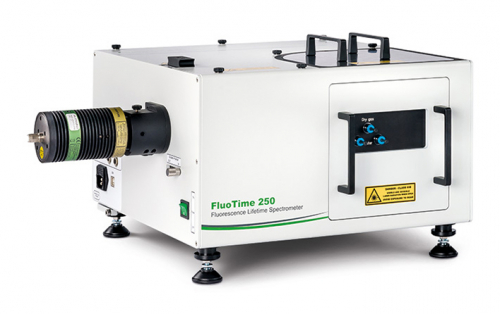
- FluoTime 250 - Compact Lifetime Fluorometer >
- MicroTime 100 - Compact Upright Photoluminescence Microscope >
- FluoMic - Compact Upright Widefield Photoluminescence Microscope >
- MicroTime 200 - Confocal microscopic platform >
- FlexWave - Wavelength Selection Unit >
Perovskite solar cells
Metal halide perovskites are an important class of emerging semiconductors, exhibiting intriguing and often unexpected electronic properties. Perovskite solar cells have received significant research interest due to their promising combination of high efficiency, low-cost manufacturing, tunability and versatility. However, issues such as long-term stability and large-area fabrication, among others, need to be addressed for successful commercialization. On a more fundamental level, their complex charge carrier dynamics are poorly understood due to limited knowledge of defect physics and co-existence of various charge carrier recombination mechanisms.
If you want to learn about microscopic time-resolved photoluminescence techniques to study defects and carrier diffusion in perovskites, request the recordings of our recent webinars:
- Prof. Jinsong Huang and Dr. Zhenyi Ni, Microscopic Study of Defects in Metal Halide Perovskites
- Prof. Sam Stranks, Multimodal microscopy of halide perovskite solar cells
Characterization of carrier recombination with time-resolved photoluminescence spectroscopy
 Tinghuan Yang, Lili Gao, and colleagues from the group of Shengzhong Liu and Kui Zhao at Shaanxi Key Laboratory for Advanced Energy Devices, together with colleagues from Wenming Tian's group at Dalian National Laboratory for Clean Energy, recently developed a one-stone-for-two-birds strategy to easily fabricate high-performance perovskite solar cells with increased long-term stability. Their key ingredient is 3API.
To characterize the optoelectronic properties of the enhanced material film, they measured the steady-state photoluminescence spectra and time-resolved photoluminescence intensity with a FluoTime 300 spectrometer. The increased PL intensity together with the longer TRPL decay suggest that 3API suppresses non-radiative carrier recombination.
Read the paper published in Nature Communications: One-stone-for-two-birds strategy to attain beyond 25% perovskite solar cellsto
Time-resolved photoluminescence imaging of layer morphology

Seul-Gi Kim and colleagues from Suwon in South Korea and Bayreuth in Germany synthesized micro-wrinkled perovskite layers. They could control the wrinkled morphology through the material composition, based on their understanding of the wrinkling mechanism.
The researcher characterized their new wrinkled perovskite and found altered photovoltaic properties compared to flat perovskite films, in particular enhanced photocurrents. Using a
MicroTime 200 time-resolved confocal microscope, they recorded TRPL maps of the photocarriers. These show clear lifetime differences between hill and valley sites.
If you are interested in the detailed mechanism underlying the microscopic wrinkle-driven enhancement of photocurrents, check out their paper published in Nature Communications: How antisolvent miscibility affects perovskite film wrinkling and photovoltaic properties
Mapping photoluminescence quantum yield
 Classical textbook theories of charge recombination are often used to describe metal halide perovskites, even though these new semiconductors often exhibit complex, unexpected electronic properties.
Are Shockley-Read-Hall and ABC models valid for lead halide perovskites? The group of Ivan Scheblykin developed a new technique for mapping photoluminescence quantum yield to find out.
The researchers mapped the photoluminescence quantum yield as a function of both excitation pulse energy, varied over 4 orders of magnitude, and pulse repetition frequency, which was tuned across a broad range from 100 Hz to 80 MHz. This was made possible by a 485 nm pulsed laser diode driven by the Sepia PDL 828 controller, run by a homemade software in a fully automated hands-off regime. The obtained results allow a detailed quantitative comparison between experiment and theory, thus testing the theoretical model's validity.
Read the paper pubslished in Nature Communications to learn more: Are Shockley-Read-Hall and ABC models valid for lead halide perovskites?
PicoQuant solutions to investigate solar cells and photovoltaics:
- Micro-photoluminescence Upgrade - Microscope-spectrometer coupling >
- FluoTime 300 - High-End Photoluminescence Spectrometer >
- FluoTime 250 - Compact Lifetime Fluorometer >
- MicroTime 100 - Compact Upright Photoluminescence Microscope >
- FluoMic - Compact Upright Widefield Photoluminescence Microscope >
- MicroTime 200 - Confocal microscopic platform >
- FlexWave - Wavelength Selection Unit >
Cadmium Telluride solar cells
Polycrystalline Cadmium Telluride, often referred to as pc-CdTe, is a semiconductor material that has gained significant attention and recognition in the field of photovoltaics, particularly in the development of solar cells. pc-CdTe solar cells are known for their cost-effectiveness, as they can be produced using relatively inexpensive manufacturing processes and easily processed.
The charge carrier lifetime is a crucial material parameter, whose lateral and transversal distribution on the surface and in the bulk can be determined by the analysis of TRPL measurements. Repeated TRPL imaging sheds light on the influence of the employed deposition technique, activation treatment, and more.
We thank H. Hempel and C. Kraft from the Dept. of Physics, University of Jena, Germany, for the CdTe waver sample.
Influence of activation step studied by TRPL imaging

A CdTe-polycrystalline wafer surface was scanned on the MicroTime 200 time-resolved confocal microscope with a pulsed 635 nm excitation laser before and after thermal activation with a chloride compound. The respective intensity images in the 814 nm to 870 nm spectral range as well as the lifetime images before and after treatment show a significant increase in intensity and photoluminescence lifetime after activation. With only a 3 ms/pixel measurement time, a distinctive change in the average lifetime can be observed as well as significant variations of the lifetime over different regions of the CdTe structure.
Read the paper in Journal of Applied Physics to learn more: Spatially resolved measurements of charge carrier lifetimes in CdTe solar cells
Behavior of charge carriers near pn-junction observed by TRPL imaging
 Intensity and luminescence image as well as carrier lifetimes of an activated PVD-grown sample were recorded in cross section configuration with a MicroTime 200 time-resolved confocal microscope. They show the decay behavior of the charge carriers, revealing a lifetime increase from the air interface to the pn-junction. Bright areas do not necessarily have the longest lifetime.
PicoQuant solutions to investigate solar cells and photovoltaics:
- Micro-photoluminescence Upgrade - Microscope-spectrometer coupling >
- FluoTime 300 - High-End Photoluminescence Spectrometer >
- FluoTime 250 - Compact Lifetime Fluorometer >
- MicroTime 100 - Compact Upright Photoluminescence Microscope >
- FluoMic - Compact Upright Widefield Photoluminescence Microscope >
- MicroTime 200 - Confocal microscopic platform >
- FlexWave - Wavelength Selection Unit >