
Materials Science
Semiconductor Characterization
Quantum Well Wafer Dynamics in Optoelectronics and Semiconductor Devices
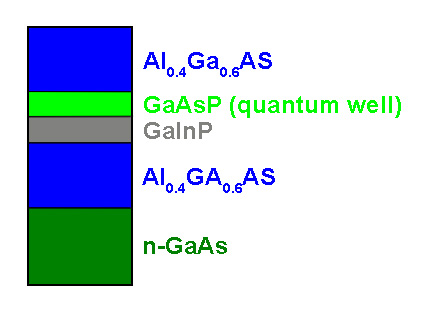
A quantum well wafer is a specialized semiconductor structure used in the fields of optoelectronics and semiconductor devices. It consists of a thin layer of a semiconductor material, in this case GaAsP, sandwiched between two thicker layers of a different semiconductor material, in this case AlGaAs. The key feature of the quantum well layer is that it's thickness of a few nanometers confines the motion of electrons in one dimension, which leads to quantized energy levels that result in several unique properties. These enable for example creation of lasers with specific wavelengths or enhancement of photodetector efficiency. The motion of free electrons, i.e. the charge carrier dynamics, can be observed with TRPL measurements.
We thank Andrea Knigge from the Ferdinand-Braun Institute in Berlin, Germany for the quantum well sample.
 Contact us
Spectrally resolved TRPL measurements separate contributions from different layers
 The quantum well sample was excited with a pulsed 595 nm excitation laser (LDH-P-FA-595) and the PL signal was recorded with a FluoTime 300 time-resolved spectrometer in the range from 630 nm to 900 nm. The time-resolved emission spectrum (TRES) clearly separates the signal contributions originating from different layers in the sample. The first peak at 650 nm stems from the Al0.4Ga 0.6As-barrier, the peak around 735 nm from the GaAsP quantum well, and the peak around 860 nm from the n-GaAs layer and the GaAs substrate. Each spectral channel can be described with a three-component exponential model. The average lifetime and the longest component of the fits are displayed. The measurement exemplifies the correlation of characteristic charge carrier dynamics in material-specific spectral channels of the multi-component system.
Read the paper in Journal of Applied Spectroscopy to learn more: Characterization of semiconductor devices and wafer materials via sub-nanosecond time-correlated single-photon counting
Excitation spectra detect layer-to-layer interactions
 Excitation spectra were recorded with a FluoTime 300 time-resolved spectrometer, using a Xe-lamp excitation with monochromator from 450 nm to 850 nm. Shown below are the excitation spectra of the 650 nm peak of the Al0.4 Ga0.6 As barrier (blue, 650 nm), of the quantum well layer with the drop around 650 nm indicating the interaction with the barrier layer (light green, 735 nm), and of the n-GaAs layer and GaAs substrate with the increase around 650 nm correlating with the absorption edge in the barrier at wavelengths longer than the barrier band gap (dark green, 860 nm). The rectangles illustrate the band gaps of the corresponding layers.
Such excitation spectra can help to determine the optimal conditions for investigations of a layer of interest.
Excitation intensity-dependent TRPL shows saturation behavior of free charge carrier dynamics
 The injection levels of free charge carriers that result from different excitation intensities offer further insight into the system specific behavior of the charge carrier dynamics. Particular contributions to the charge carrier lifetime are intrinsically intensity dependent and can be differentiated from other contributions to the total charge carrier lifetime by varying the intensity in the photoexcitation.
To limit the excitation to a defined area of about 100 µm diameter, the time-resolved photoluminescence above 665 nm was measured with a MicroTime 100 time-resolved confocal microscope using a 635 nm pulsed excitation laser.
The saturation effect in the average lifetime obtained from the TRPL curves is visible when plotting the lifetime versus excitation intensity, as the lifetime approaches a fixed value.
Carrier diffusion directly observed by TRPL imaging

Charge carrier diffusion can be directly observed by TRPL imaging. The sample was excited at the central spot of the image with a pulsed 440 nm laser and PL signal was detected in the 710 nm to 760 nm range using an LSM upgrade kit. Note that only the detection volume was scanned to create the TRPL image. Analysis of individual regions of interest (ROI) with increasing diameter shows that the average lifetime increases for larger distances from the excitation spot due to a rising component. This stems from the longer time that charge carriers need to diffuse from the center to the selected ROI before recombining and emitting a photon. Further analysis would yield the diffusion time.
 PicoQuant solutions to investigate semiconductors:
