
Materials Science
Characterization of Nanomaterials and 2D Materials
Quantum Dots, Carbon Dots, TMDs
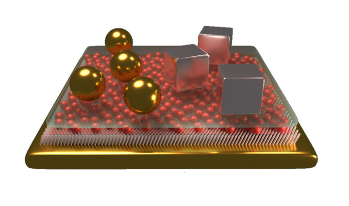
Nanomaterials, including nanoparticles and 2D materials, are unique due to their remarkable physical, chemical, and electronic properties that emerge at the nanoscale because of quantum confinement. For example, they can scatter, absorb, or emit light differently from bulk materials. 2D materials like graphene have excellent electron transport properties, making them attractive for next-generation electronic devices and transparent conductive films.
The properties of nanomaterials can be finely tuned by adjusting their size, shape, or composition. This tunability is essential for tailoring them to specific applications, from electronics to catalysis. Working with nanomaterials also presents challenges, and TRPL is one of the characterization techniques that can address these challenges.

Webinar: Designer van der Waals Materials for Quantum Optical Emission
The session explores how engineered 2D materials like TMDs are enabling breakthroughs in quantum photonics. It features advanced techniques such as time-resolved photoluminescence and spectroscopy to analyze emission behavior.
Presenter: Shengxi Huang, Rice University — a leading researcher in quantum materials and optical sensing.
Request full video to learn more >
 Contact us
Carbon dots
Carbon dots, which are small carbon nanoparticles, have gained significant attention in recent years due to their versatile properties. One of their most notable features is a strong and tunable photoluminescence across the visible and NIR spectrum. They also exhibit good electrical conductivity, making them attractive for optoelectronic devices and light-emitting diodes.
Complexes of carbon dots and plasmonic metal nanoparticles with enhanced emission

When carbon dots and plasmonic metal nanoparticles form complexes, the carbon dot's absorption and emission overlaps with the plasmon resonance of the metals. For the most optimized complex architecture, this increases emission up to 5-fold.
Metal nanoparticles may on the one hand enhance PL emission of nearby emitters due to local enhancement of excitation or the acceleration of spontaneous recombination, on the other hand they may quench emission due to non-radiative decay via plasmon-induced energy transfer. The overall effect on the PL depends on many parameters, among them the nanoscale architecture. To determine the nanoscale architecture, the weight ratio of carbon dots to gold nanoparticles can be varied systematically during sample preparation. This ratio influences the number of carbon dots conjugated to nanoparticles in the resulting complexes.
PL decays were acquired on a MicroTime 100 time-resolved confocal microscope equipped with a 405 nm excitation laser. When the carbon dot/gold nanoparticle weight ratio was increased, the PL quantum yield also increased, while the PL lifetime decreased. This is probably due to PL quenching via energy transfer, enabled by the overlap between the gold nanoparticle plasmon resonance spectra and the carbon dot PL band. These observations support the determination of optimal complex architecture and composition.
To learn more, read the paper in Nanomaterials (2023): Carbon Dot Emission Enhancement in Covalent Complexes with Plasmonic Metal Nanoparticles
Carbon dots with NIR absorption and emission
 Carbon dots with NIR absorption and emission in the NIR region in aqueous solution are desirable for bioimaging applications, among others. In this work, researchers modified the surface of carbon dots with polyethyleneimine (PEI) to achieve just that. They characterized the optical properties of their new PEI-CDs, recording PL intensity and decay curves under various conditions with a MicroTime 100 time-resolved confocal microscope. PEI-modification increases the PL lifetime, probably by inhibiting energy dissipation by water molecules.
To learn more, read the paper in Advanced Science (2022): Toward Strong Near-Infrared Absorption/Emission from Carbon Dots in Aqueous Media through Solvothermal Fusion of Large Conjugated Perylene Derivatives with Post-Surface Engineering
Carbon dot/graphene hybrid white laser characterization
 For future wearable technologies such as e-skins and personal health monitors, flexible, stretchable, and lightweight optoelectronic devices are required. To this end, researchers developed a cavity-free white laser integrating fluorescent carbon dots and crumpled graphene.
To characterize the optical properties of the new device, TRPL spectra and PL decay curves of deformed and undeformed materials were recorded as a function of pumping power density, using a pulsed excitation laser at 375 nm (LDH series). These provide information on the carrier lifetimes in the material, which clearly decrease with increasing power, probably due to stimulated emission. The crumpled graphene is thought to form a virtual cavity for emitted photons by scattering.
To learn more, read the paper in Optics Express (2022): All-carbon stretchable and cavity-free white lasers
 PicoQuant solutions to investigate nanoparticles and 2D materials:
- Micro-photoluminescence Upgrade - Microscope-spectrometer coupling >
- FluoTime 300 - High-End Photoluminescence Spectrometer >
- FluoTime 250 - Compact Lifetime Fluorometer >
- MicroTime 100 - Compact Upright Photoluminescence Microscope >
- FluoMic - Compact Upright Widefield Photoluminescence Microscope >
- MicroTime 200 - Confocal Microscopic Platform >
- Wavelength Selection Unit FlexLambda >
Perovskite nanostructures
 and 3D film (DEP)") Methylammonium lead iodide (MAPbI3) perovskite films are used as light absorbers in solar cells. Recently, 1D nanowire perovskites were reported to have better properties than the usually employed 3D bulk material, but it was not clear why. To find out, researchers from the group of Man-Jong Lee developed a new technique for the reproducible synthesis of both 1D and 3D perovskites with the same composition but different dimensions. The key is an antisolvent washing step with dibutyl ether (DB) or diethyl ether (DE). Perovskite layers washed with DB and DE are designated as DBP and DEP, respectively. DBP consists of interconnected perovskite nanowires, whereas DEP is a 3D film.
Methylammonium lead iodide (MAPbI3) perovskite films are used as light absorbers in solar cells. Recently, 1D nanowire perovskites were reported to have better properties than the usually employed 3D bulk material, but it was not clear why. To find out, researchers from the group of Man-Jong Lee developed a new technique for the reproducible synthesis of both 1D and 3D perovskites with the same composition but different dimensions. The key is an antisolvent washing step with dibutyl ether (DB) or diethyl ether (DE). Perovskite layers washed with DB and DE are designated as DBP and DEP, respectively. DBP consists of interconnected perovskite nanowires, whereas DEP is a 3D film.
Jung et al. characterized both materials, using TRPL with their MicroTime 200 time-resolved confocal microscope to measure the charge-carrier lifetimes, transport times and charge transport dynamics in two different directions, normal and parallel to the surface. Fitting of the TRPL decays extracted from the FLIM images yielded the transport times in the ns range. The photoluminescence intensity reduction indicates fast charge extraction. Overall, they found improved charge carrier dynamics of 1D nanowire films.
To learn more, read the paper in Journal of Materials Research and Technology (2021): Antisolvent-assisted one-step solution synthesis of defect-less 1D MAPbI3 nanowire networks with improved charge transport dynamics
X-ray decay curves of a 2D-perovskite functionalized fiber-type heterostructured scintillator
2PbBr4 heterostructure. Additional fast decay components confirm the presence of several materials in the heterostructure.") For fast timing applications such as time-of-flight Positron Emission Tomography (ToF-PET), new heterostructured detectors with a matrix and a filler component working in synergy are being developed. For good detector performance, the choice of filler material is critical. In this work, a new fast scintillator based on 2D-perovskites is characterized.
For fast timing applications such as time-of-flight Positron Emission Tomography (ToF-PET), new heterostructured detectors with a matrix and a filler component working in synergy are being developed. For good detector performance, the choice of filler material is critical. In this work, a new fast scintillator based on 2D-perovskites is characterized.
X-ray decay curves were measured with a PMA-C PMT detector and a TCSPC module. The 2D-perovskite functionalized material (blue) shows an additional fast decay component compared to the bismuth germanate matrix (grey), proving the presence of perovskite.
To learn more, read the paper: Applied Physics Letters (2023): Two-dimensional perovskite functionalized fiber-type heterostructured scintillators
PicoQuant solutions to investigate nanoparticles and 2D materials:
- Micro-photoluminescence Upgrade - Microscope-spectrometer coupling >
- FluoTime 300 - High-End Photoluminescence Spectrometer >
- FluoTime 250 - Compact Lifetime Fluorometer >
- MicroTime 100 - Compact Upright Photoluminescence Microscope >
- FluoMic - Compact Upright Widefield Photoluminescence Microscope >
- MicroTime 200 - Confocal Microscopic Platform >
- Wavelength Selection Unit FlexLambda >
2D Transition metal disulfides and dichalcogenides
Evaluating chemical treatment for TMDs with confocal TRPL and exciton diffusion
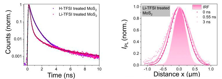
Zhaojun Li and colleagues work towards high performance optoelectronic devices made of 2D materials based on semiconducting transition metal disulfides (TMDs). Some chemical treatments improve the photoluminescence (PL) yield of these materials much more than others, but the reason why is so far unknown.
To elucidate the mechanism of the PL enhancement of H-TFSI-treated and Li-TFSI-treated monolayer MoS2 samples, the team performed confocal TRPL with their MicroTime 200 time-resolved confocal microscope, equipped with a pulsed 405 nm excitation laser, among other techniques.
They observed a decrease in lifetime with an increase in PL intensity, indicating higher radiative recombination rates after chemical treatment. The decay dynamics are noticeably different upon Li- and H-TFSI-treatment.
Moreover, exciton transport is observable with confocal TRPL by exciting a central spot and then imaging the surrounding area. From the broadening of the spatial profile of the normalized PL intensity over several ns, they obtained the exciton diffusion coefficients. It turns out that excitons propagate more efficiently in the Li-TFSI-treated sample.
To learn more, read the paper in Nature Communications (2021): Mechanistic insight into the chemical treatments of monolayer transition metal disulfides for photoluminescence enhancement
SHG, TRPL, and TPE-TRPL imaging of TMDs monolayers
 2D monolayers of transition metal dichalcogenides (TMDs) have interesting electrooptical properties for various applications such as flexible electrodes for wearable electronics.
Here, 2D monolayers MoS2 and WSe2 on PDMS were imaged with several complementary techniques, namely reflection, SHG, TRPL imaging and TPE imaging using a single microscope, the MicroTime 100 time-resolved confocal microscope. Thus, the optical properties of the materials could be characterized locally with several techniques to obtain a comprehensive understanding.
The MicroTime 100 was equipped with a pulsed 640 nm laser (LDH-P-C-640B) for TRPL imaging and a pulsed 1064 nm laser (VisIR 1064) for SHG imaging and TRPL imaging with two-photon excitation (TPE), as well as a camera for reflection imaging.
We thank Jin Myung Kim from UC Irvine for the samples.
Download our poster to learn more: Second-Harmonic Generation (SHG) Imaging Microscopy with ps Pulsed Lasers
PicoQuant solutions to investigate nanoparticles and 2D materials:
- Micro-photoluminescence Upgrade - Microscope-spectrometer coupling >
- FluoTime 300 - High-End Photoluminescence Spectrometer >
- FluoTime 250 - Compact Lifetime Fluorometer >
- MicroTime 100 - Compact Upright Photoluminescence Microscope >
- FluoMic - Compact Upright Widefield Photoluminescence Microscope >
- MicroTime 200 - Confocal Microscopic Platform >
- Wavelength Selection Unit FlexLambda >